Manchester, EPFL and ENS Lyon teams image how nanochannel deformation stores ionic memory

Source: https://www.nature.com/articles/s41563-026-02775-4
 Kalluvadi Veetil Saurav
At a glance
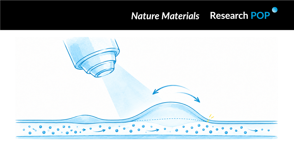
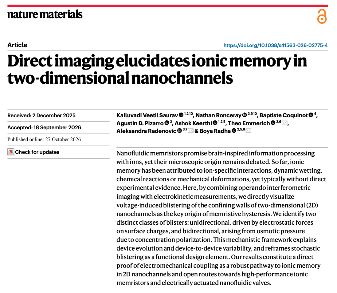
An ionic channel can respond differently to the same voltage depending on its recent history. Researchers from the University of Manchester, EPFL, ENS Lyon and the Institute of Science and Technology Austria directly image a structural change associated with this memory: nanoscale blisters in the channel walls.
By synchronizing interferometric microscopy with electrical measurements, the team observed wall displacements approximately 5–25 nm high that appeared alongside abrupt conductance changes. Measurements of 50 blisters across nine devices revealed two response classes, which the authors connect to osmotic and electrostatic pressures.
Adhesion between the layers provides the proposed memory mechanism. Because opening and closing a blister follow different paths, the channel geometry—and therefore its conductance—depends on its voltage history.
Background
Ions carry electrical current through aqueous channels. When those channels become extremely narrow, their walls strongly influence transport: surface charge affects the local ion population, confinement changes the molecular environment, and small geometric variations can alter the available conducting pathways.
An applied voltage can also redistribute ions unevenly. This concentration polarization creates regions with different salt concentrations and can generate pressure differences within the device. If the channel walls are mechanically compliant, those forces may change the channel itself.
Such feedback offers a possible explanation for conductance hysteresis, in which current follows different branches as voltage is swept forward and backward. Hysteresis is relevant to ionic memory and neuromorphic devices because it indicates that the system retains information about previous conditions. An electrical curve, however, does not reveal what physical feature stores that information.
The study addresses this gap by observing channel deformation during electrical operation. It asks whether changes in wall shape provide a measurable link between ionic redistribution and the device’s history-dependent response.
Research question
Does conductance hysteresis coincide with deformation of two-dimensional nanochannel walls? Which forces explain blisters that respond to both voltage polarities and those that favor one polarity? How does interlayer adhesion allow the resulting geometry to retain a memory of earlier conditions?
Inside the study
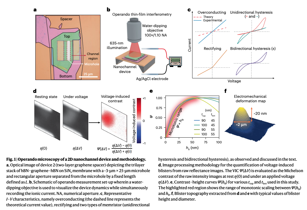
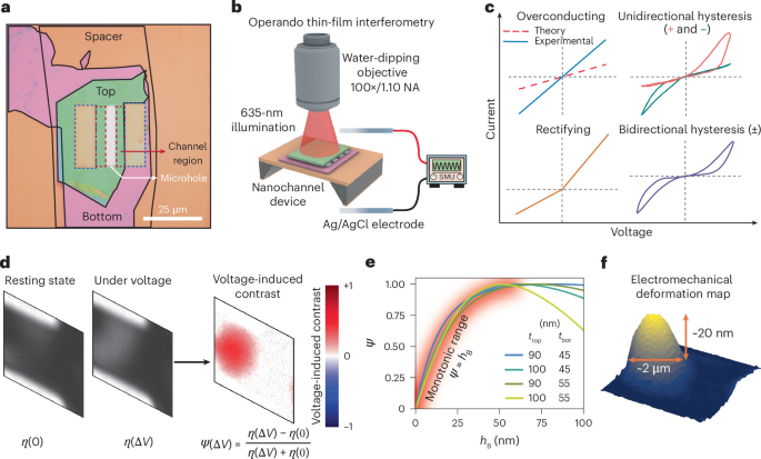
The experimental approach in Figure 1 combines a layered nanofluidic device with simultaneous optical and electrical measurements. Materials including hexagonal boron nitride and graphite form confined aqueous channels. Interferometric microscopy detects voltage-induced changes in reflected light, which are calibrated to estimate local blister heights.
This method makes wall displacements of approximately 5–25 nm accessible during operation. Recording current at the same time allows the researchers to compare changes in conductance with the appearance and evolution of individual deformations.
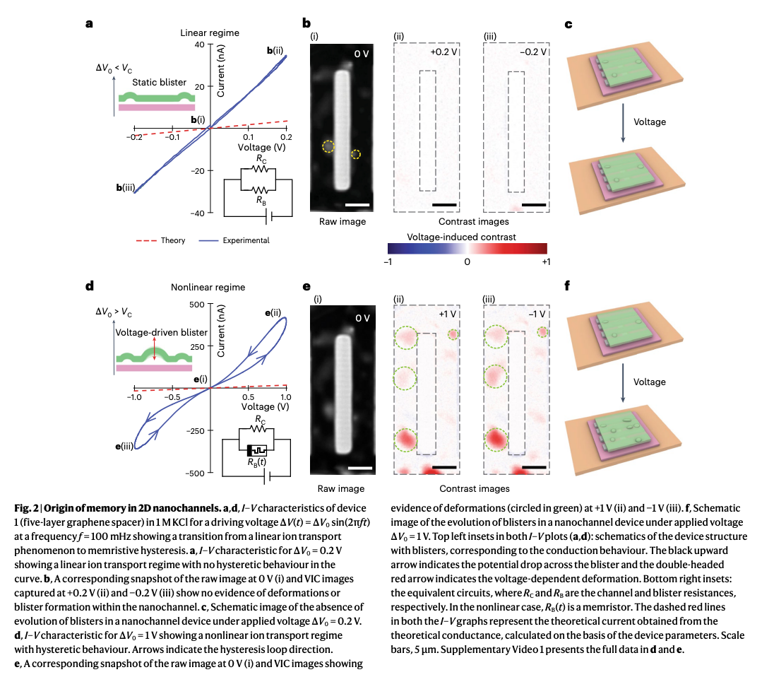
The connection becomes clear during voltage sweeps. As shown in Figure 2, abrupt conductance jumps coincide with local delamination and blister growth. When the voltage sweep reverses, the walls do not immediately retrace their earlier structural path, and the current follows a different branch.
These observations identify wall geometry as a physical state variable associated with ionic memory. At a given applied voltage, the channel may contain a different arrangement of adhered and blistered regions depending on its previous exposure. That structural difference can change the measured conductance.
Spatiotemporal imaging follows how individual blisters nucleate, expand and recede. Their locations and switching times vary, indicating that deformation begins unevenly across the device. The authors relate this variability to local differences in adhesion, charge and ion-transport pathways.
A blister’s electrical influence also depends on where it forms. Deformation near a major conducting pathway can have a greater effect on total current than a conspicuous blister elsewhere. The optical and electrical measurements therefore provide complementary information: blister visibility alone does not determine its contribution to conductance.
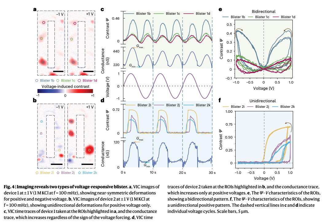
The comparison in Figures 4 and 5 extends the analysis to 50 blisters in nine devices. Some blisters develop under both positive and negative bias, while others appear predominantly under one polarity. The measured responses cluster into two symmetry classes, giving the mechanical model two distinct behaviors to explain.
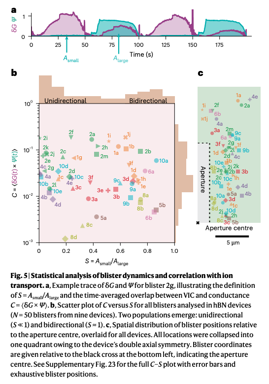
For the bidirectional class, the authors propose osmotic pressure generated by concentration polarization. Voltage-driven ion redistribution creates concentration differences that can exert pressure on the channel walls. Because this redistribution can occur under either voltage direction, blister formation can occur at both polarities.
For the polarity-selective class, the proposed driving force is electrostatic pressure acting on charged surfaces. Its mechanical effect depends on the direction of the electric field, providing a route to deformation that favors one bias polarity.
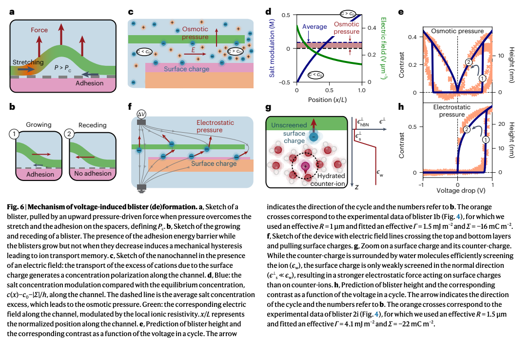
The model in Figure 6 combines these pressure sources with interlayer adhesion. Pressure can promote separation, but creating a blister requires overcoming the energetic cost of detaching adjacent layers. Once formed, the blister can persist along a different path as the driving force decreases.
This difference between opening and closing supplies the proposed memory barrier. The instantaneous voltage determines part of the force acting on the walls, while the existing deformation and adhesion state influence how they respond. Ion transport, pressure and geometry consequently evolve together.
Takeaways and outlook
The study connects an electrical memory signature to directly observed structural changes. Blister formation accompanies conductance jumps, while the different paths followed during growth and retreat explain how channel geometry can retain information about earlier voltage conditions.
The distinction between osmotic and electrostatic driving forces also suggests ways to investigate control. Surface charge, interlayer adhesion and the placement of compliant regions could be varied to test whether blister formation can become more predictable.
The present work establishes an electromechanical explanation under the studied conditions. Developing practical ionic memory devices will require reproducible switching, controlled states and sustained operation across repeated cycles. The imaging approach provides a way to examine those requirements while observing the physical structure responsible for the electrical response.
About the researchers
Kalluvadi Veetil Saurav of the University of Manchester and Nathan Ronceray of EPFL contributed equally. Theo Emmerich of ENS Lyon, Aleksandra Radenovic of EPFL and Boya Radha of the University of Manchester are the corresponding authors.
Baptiste Coquinot is affiliated with the Institute of Science and Technology Austria. Agustin D. Pizarro is affiliated with EPFL, and Ashok Keerthi with the University of Manchester.
Original research
Kalluvadi Veetil Saurav; Nathan Ronceray; Baptiste Coquinot; Agustin D. Pizarro; Ashok Keerthi; Theo Emmerich; Aleksandra Radenovic; Boya Radha. “Direct imaging elucidates ionic memory in two-dimensional nanochannels.” Nature Materials. Published online 27 October 2026.
Original paper: https://doi.org/10.1038/s41563-026-02775-4
Research POP Notes
This article reflects the independent interpretation of the Research POP team and does not represent the views of the authors, their institutions or the journal. If you identify any inaccuracies or have concerns regarding the content, figures or attribution, please contact us at team.researchpop@gmail.com. We will review the matter promptly and make corrections or remove the relevant material where appropriate.