Empa and ETH Zurich researchers map what makes wide-bandgap perovskite films emit more strongly

Source: https://advanced.onlinelibrary.wiley.com/doi/10.1002/adfm.77319
At a glance
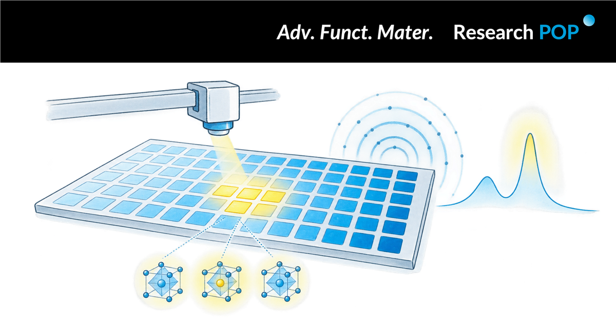
Why do some wide-bandgap perovskite films emit more strongly than others? Researchers at Empa and ETH Zurich prepared and characterized 569 samples using combinatorial vapor deposition, independently varying the cesium-to-lead and bromide-to-chloride ratios. A Cs/Pb range of approximately 1.05–1.20 showed elevated relative photoluminescence, while an optical feature near 3.4 eV accompanied the brighter films. The study connects high-throughput composition mapping with structural and spectroscopic measurements to provide a practical route for screening wide-bandgap materials.
The researchers examine how thin-film composition, structure and optical response change across a large materials library. By combining automated synthesis and multimodal characterization, they identify both a promising compositional range and an optical signature associated with stronger emission.
Background
Lead-halide perovskites can be tuned by changing their elemental composition. Wide-bandgap members of this family are relevant to applications requiring higher-energy photons, but the large number of possible compositions makes one-recipe-at-a-time optimization slow. Composition also influences how a film forms, linking its optical response with crystal structure and local chemical environment.
The team focused on inorganic films containing cesium, lead, bromide and chloride. Sequential physical vapor deposition allowed the cesium-to-lead ratio to be varied independently from the bromide-to-chloride ratio. Automated measurements then connected each sample's composition with diffraction, photoelectron spectroscopy, absorption and photoluminescence data.
Research question
The study examines which regions of the Cs/Pb and Br/Cl compositional space produce stronger emission and whether an additional optical feature can help identify the same films. The researchers combine composition, crystal structure, local chemical environment and optical measurements to understand how these properties change together across the materials library.
Inside the study
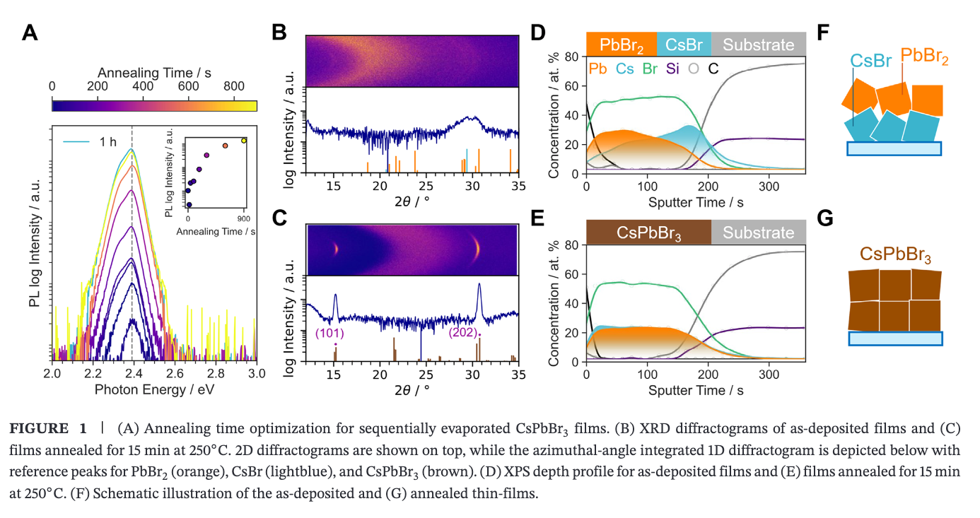
The researchers first optimized a sequential vapor-deposition process using CsPbBr3. CsBr and PbBr2 were deposited in layers and then annealed. Photoluminescence approached a plateau after approximately 15 minutes at 250 °C. During annealing, diffraction changed from precursor-like signatures to CsPbBr3 reflections, while depth-resolved photoelectron spectroscopy showed a more uniform elemental profile through the film.
The team then created spatial gradients of CsBr, with CsCl added in selected libraries, followed by a uniform PbBr2 layer and annealing. Each materials library contained 44 defined sample positions. Across several libraries, the study covered 569 samples spanning different Cs/Pb and Br/Cl ratios. X-ray diffraction tracked crystal structure, X-ray photoelectron spectroscopy measured composition and chemical state, and absorption and photoluminescence characterized the optical response.
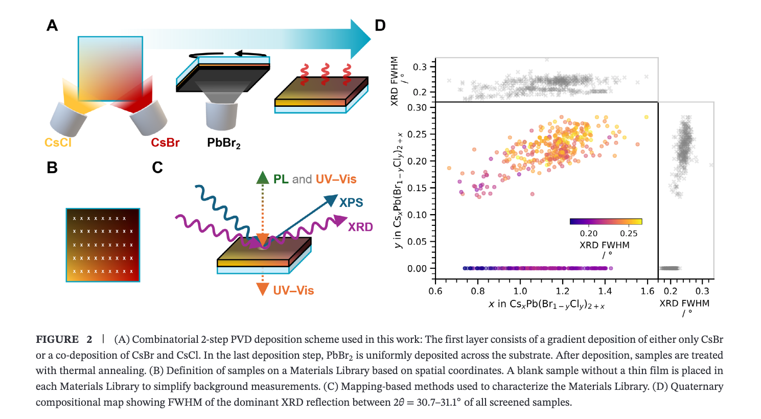
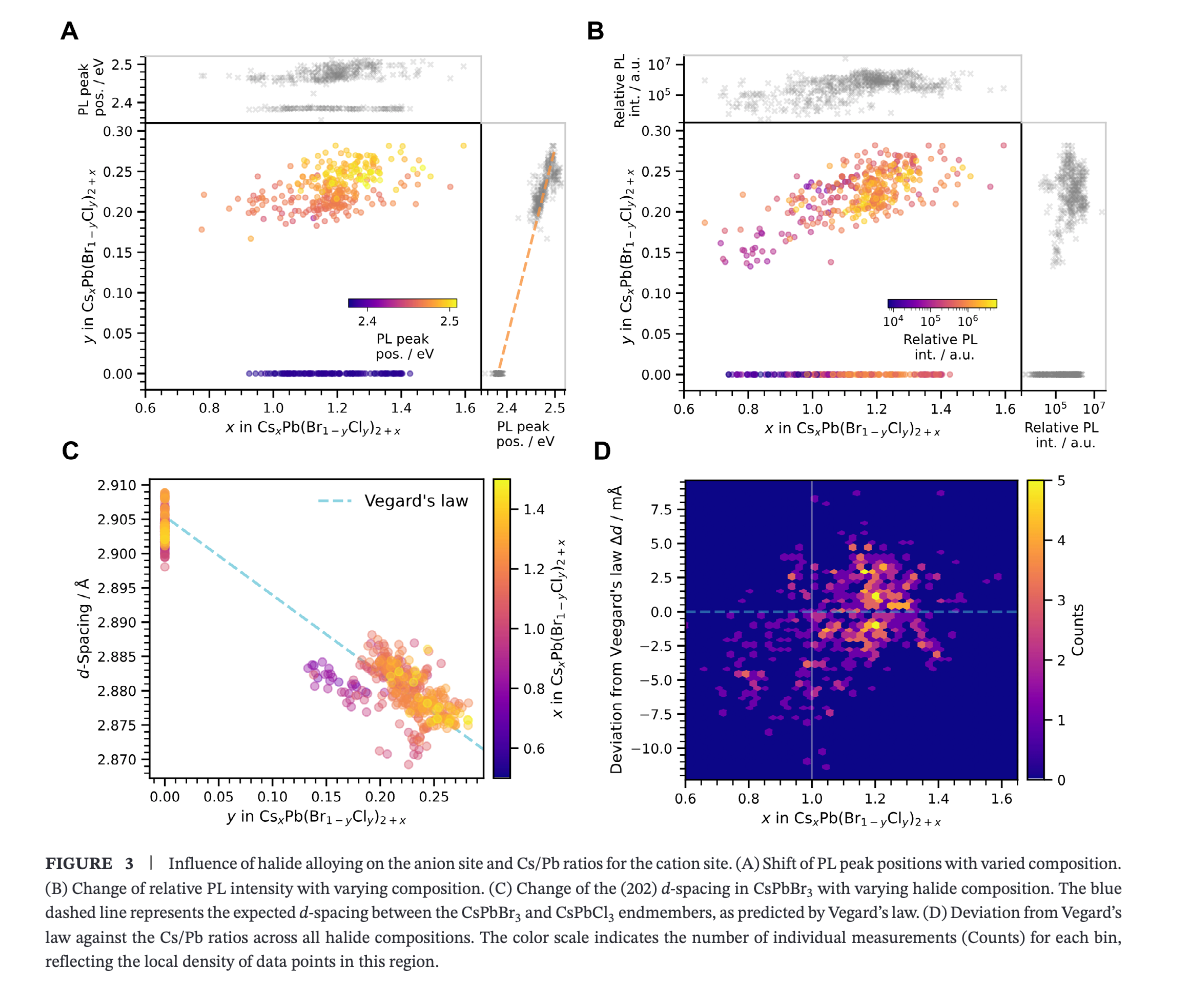
Introducing chloride shifted the photoluminescence peak, reflecting the change in halide composition. The absorption-corrected relative photoluminescence intensity varied particularly strongly with Cs/Pb. The mapped data showed a high-response region around Cs/Pb 1.1–1.2, which the authors describe more broadly as a practical compositional window of approximately 1.05–1.20.
X-ray diffraction provided a structural view of the same materials space. At a given Cs/Pb ratio, the lattice spacing broadly followed the trend expected from bromide-chloride alloying, while the deviations changed systematically with Cs/Pb. The more emissive compositions appeared in a region with smaller deviations, connecting the photoluminescence response with the structural evolution of the films.
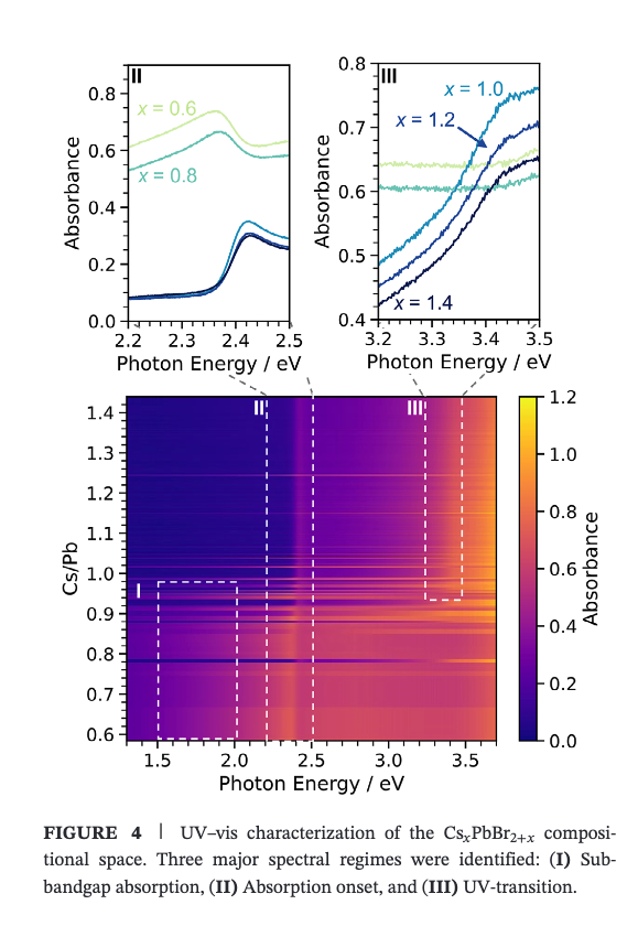
Absorption spectroscopy revealed three recognizable energy regions in the Cs–Pb–Br series: a sub-bandgap response, an absorption onset near 2.4 eV and a higher-energy feature near 3.4 eV. The sub-bandgap response was more evident in cesium-poor films, while the ultraviolet feature became more prominent in slightly cesium-rich compositions.
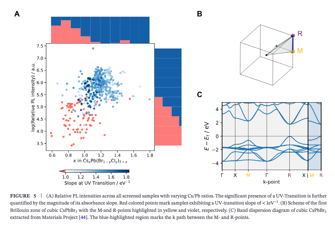
When the full dataset was analysed together, a more pronounced slope associated with the ultraviolet transition accompanied higher relative photoluminescence. This relationship was especially informative near Cs/Pb around 1, where the samples displayed a broad range of emission intensities. The authors assign the feature to an optical transition associated with the M point of the CsPbBr3 Brillouin zone, based on the band-dispersion picture and earlier optical studies.
X-ray photoelectron spectroscopy added a local chemical perspective. The relative difference between bromine and lead core-level binding energies changed with Cs/Pb and reached a maximum near 1.1, close to the composition range with stronger relative emission. The authors connect this trend with the nearest-neighbour geometry around lead and bromine, including octahedral tilting and short-range structural order.
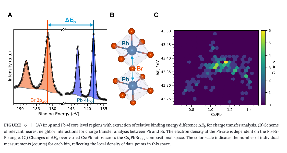
Together, the measurements trace a continuous relationship across the library. Controlled synthesis defines the compositional space, photoluminescence identifies the higher-response region, the ultraviolet transition provides an additional optical descriptor, and diffraction and photoelectron spectroscopy connect these signals with structural and local chemical changes.
Takeaways and outlook
The study identifies a Cs/Pb window of approximately 1.05–1.20 associated with elevated relative photoluminescence in the wide-bandgap perovskite films. It also highlights a higher-energy optical feature near 3.4 eV that tracks the more emissive samples and can be measured using standard absorption spectroscopy.
The broader contribution is a high-throughput workflow that links synthesis, composition, crystal structure and optical response across hundreds of samples. Rather than optimizing one composition at a time, the approach maps how several material properties evolve together and provides measurable descriptors for selecting promising regions. Future work can build on these film-level relationships when developing materials for specific optoelectronic devices.
About the researchers
Alexander Wieczorek (Empa)
Sergey Tsarev (Empa; ETH Zurich)
Nathan Rodkey (Empa)
Oleksandr Pshyk (Empa)
Stefanie Frick (Empa)
Maksym V. Kovalenko (Empa; ETH Zurich)
Sebastian Siol (Empa; corresponding author)
Original research
Alexander Wieczorek, Sergey Tsarev, Nathan Rodkey, Oleksandr Pshyk, Stefanie Frick, Maksym V. Kovalenko and Sebastian Siol. “Tuning the Optoelectronic Properties of Wide Bandgap Perovskites: Data-Driven Insights from Combinatorial Synthesis and High-Throughput Experimentation.” Advanced Functional Materials, published online 17 September 2026. DOI: 10.1002/adfm.77319.
Open access publishing facilitated by ETH-Bereich Forschungsanstalten, as part of the Wiley - ETH-Bereich Forschungsanstalten agreement via the Consortium Of Swiss Academic Libraries.
Research POP Notes
This article reflects the independent interpretation of the Research POP team and does not represent the views of the authors, their institutions or the journal. If you identify any inaccuracies or have concerns regarding the content, figures or attribution, please contact us at team.researchpop@gmail.com. We will review the matter promptly and make corrections or remove the relevant material where appropriate.