Nanjing University-led team controls 2.0-eV perovskite crystallization for 30.1% triple-junction efficiency


Source: https://www.nature.com/articles/s41560-026-02135-1
At a glance
All-perovskite triple-junction solar cells use three absorbers with different bandgaps, allowing each layer to use a different part of the solar spectrum. The approximately 2.0 eV Br-rich perovskite at the top of the stack is particularly demanding. Surface wrinkling, uneven Br/I distributions and non-radiative recombination can limit the voltage and current of the complete series-connected device.
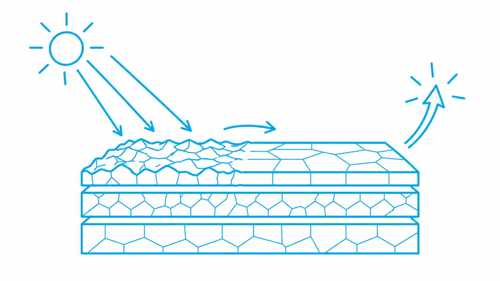
A Nanjing University-led team focused on how this top film crystallizes after its initial deposition. The researchers applied a surface reconstruction and halide homogenization treatment to FA₀.₇Cs₀.₃PbIBr₂ films. The treatment used HFIP and DMF at a 30:1 volume ratio, with 1 mg mL⁻¹ oleylammonium chloride (OAmCl). The root-mean-square surface roughness decreased from 110.0 to 63.9 nm, while the time-resolved photoluminescence lifetime increased from 23.1 to 110.1 ns.
The champion treated ultrawide-bandgap single-junction cell reached a power-conversion efficiency of 15.2%. When the material was incorporated into a 0.049 cm² monolithic all-perovskite triple-junction cell, the champion device reached a reverse-scan efficiency of 30.1%. Across 35 treated triple-junction devices, the average efficiency was 29.6 ± 0.3%, compared with 28.0 ± 0.3% for the controls. The paper separately reports an independently certified reverse-scan efficiency of 29.3%.
Background
A triple-junction solar cell stacks three absorbers with different bandgaps. Higher-energy photons are absorbed near the top, while the middle and bottom subcells collect other parts of the solar spectrum. Because the three subcells are connected in series, the electrical performance of the approximately 2.0 eV top absorber affects the output of the complete device.
Increasing the bromide content helps create this ultrawide bandgap, but the paper identifies several related challenges. Rapid crystallization can produce surface wrinkles, lateral variations in bromide and iodide distribution, local bandgap fluctuations and recombination pathways that reduce the voltage available from the absorber.
The team’s strategy was to reconstruct the film surface immediately after the conventional antisolvent step, giving the still-wet material a controlled opportunity to reorganize instead of treating the completed film only with an additional passivation layer.
A mixture of hexafluoroisopropanol (HFIP) and a small proportion of N,N-dimethylformamide (DMF) induces partial surface dissolution and limited reflow. Chloride supplied by OAmCl participates temporarily in intermediate phases during crystallization and is then largely removed during annealing. The authors propose that this transient chloride participation helps synchronize bromide and iodide incorporation, producing a more homogeneous mixed-halide film.
Research question
Can controlled surface reconstruction, combined with transient chloride participation, reduce wrinkling and halide heterogeneity in approximately 2.0 eV perovskites and translate those film-level changes into higher voltage, efficiency and stability in complete all-perovskite triple-junction solar cells?
The study follows this question from material formation to device performance. It examines crystal structure, surface morphology, surface potential, halide distribution, recombination, charge transport, ultrawide-bandgap single-junction cells, monolithic triple-junction cells and three stability protocols.
The measured changes support the authors’ crystallization-control mechanism. However, the detailed chloride-mediated sequence remains an interpretation based on the combined structural, compositional and device-level evidence.
Inside the study
The researchers treated spin-coated FA₀.₇Cs₀.₃PbIBr₂ films with an HFIP/DMF mixture at a 30:1 volume ratio containing 1 mg mL⁻¹ OAmCl. This combined treatment was designated HDCl. The films were subsequently annealed at 85 °C for 5 minutes and then at 135 °C for 15 minutes. Control films used the same precursor and antisolvent procedure but did not undergo the subsequent surface reconstruction and halide homogenization treatment.
X-ray diffraction showed that the full width at half maximum of the (100) peak narrowed from 0.171° in the control film to 0.149° in both the HD- and HDCl-treated films. The authors interpreted the narrower peak as evidence of improved crystallinity and a more homogeneous mixed-halide phase after annealing.
The surface also became smoother. Atomic force microscopy measured a reduction in root-mean-square roughness from 110.0 nm for the control film to 63.9 nm for the treated film.
Kelvin probe force microscopy showed that the control film had a broad work-function distribution between 5.0 and 5.2 eV. In contrast, the HDCl-treated film exhibited a much narrower distribution centred at 5.13 eV. Together with time-of-flight secondary ion mass spectrometry maps of Br and I, the narrower surface-potential distribution supports greater lateral compositional uniformity.
Optical measurements indicated lower non-radiative losses after treatment. HDCl-treated films produced approximately 1.8 times the photoluminescence intensity of the control films. The time-resolved photoluminescence lifetime increased from 23.1 to 110.1 ns. In neat films, the estimated non-radiative voltage loss decreased from 163 to 143 meV.
Charge-transport measurements pointed in the same direction. Optical-pump terahertz-probe data fitted using the Drude–Smith model gave a combined electron-and-hole mobility of 36 cm² V⁻¹ s⁻¹ for the control film and 53 cm² V⁻¹ s⁻¹ for the HDCl-treated film.
Carrier diffusion lengths calculated from the OPTP decay dynamics increased from 0.47 to 0.72 μm. These are model-extracted quantities rather than direct measurements of individual charge trajectories. Thermal admittance spectroscopy, transient photovoltage measurements and impedance spectroscopy provided additional evidence of reduced trap-assisted recombination.
The champion treated ultrawide-bandgap single-junction cell delivered a power-conversion efficiency of 15.2%, compared with 14.2% for the control. The open-circuit voltage increased from 1.40 to 1.46 V, while the fill factor increased from 80.4% to 82.3%.
The champion device maintained a stabilized efficiency of 15.1% during 600 seconds of maximum-power operation. Its external quantum efficiency spectrum produced an integrated photocurrent density of 12.6 mA cm⁻². Across 35 independently fabricated treated cells, the average efficiency was 15.0%.
The current density–voltage measurements used a 0.049 cm² active area defined by an aperture mask, an illumination intensity of 100 mW cm⁻² and a scan rate of 10 mV s⁻¹.
For the monolithic triple-junction device, the champion reverse scan produced a power-conversion efficiency of 30.1%, with an open-circuit voltage of 3.521 V, a short-circuit current density of 10.9 mA cm⁻² and a fill factor of 78.4%. Its forward-scan efficiency was 29.9%.
Across 35 treated triple-junction devices, the average values were:
- Open-circuit voltage: 3.515 ± 0.009 V
- Short-circuit current density: 10.8 ± 0.1 mA cm⁻²
- Fill factor: 77.8 ± 0.4%
- Power-conversion efficiency: 29.6 ± 0.3%
Control triple-junction devices had an average efficiency of 28.0 ± 0.3%.
The champion device was independently certified by the Shanghai Institute of Microsystem and Information Technology. The certified reverse-scan efficiency was 29.3%, with a reported hysteresis index of 1.5%. The 30.1% value is the study’s own champion reverse-scan measurement rather than the independently certified result.
The researchers also evaluated the devices under three different stability protocols.
In the damp-heat test, encapsulated devices were stored under open-circuit conditions for 240 hours at 85 ± 2 °C and 85 ± 5% relative humidity. The treated group retained 90% of its initial efficiency, while the control group retained 50%.
In the thermal-cycling test, encapsulated devices underwent 200 cycles between −40 and 85 °C. The treated devices retained 91% of their initial efficiency, compared with 68% for the controls. The damp-heat and thermal-cycling experiments each used five devices per group, with results reported as mean ± standard deviation.
Operational stability was assessed by maximum-power-point tracking in ambient air under simulated AM1.5G illumination at 100 mW cm⁻². The ambient temperature was approximately 25 °C, while the device temperature rose to approximately 35 °C because no active cooling was used.
The treated triple-junction device retained more than 90% of its initial efficiency after 569 hours. The control device reached T90 after 246 hours. T90 refers to the time at which a device’s efficiency decreases to 90% of its initial value. The 569-hour result should therefore be described as a test duration over which the treated device remained above 90%, rather than as a precisely measured T90 value.
The paper contains three different descriptions of the middle-bandgap absorber. The Results section describes it as FA₀.₈Cs₀.₂Pb(I₀.₈Br₀.₂)₃. A Methods heading identifies it as FA₀.₈Cs₀.₂Pb(I₀.₉Br₀.₁)₃, while the corresponding preparation recipe gives a PbI₂/PbBr₂ molar ratio of 0.85:0.15. This summary notes the reporting difference rather than selecting one composition as definitive.
Takeaways and outlook
The study links a post-deposition crystallization treatment to a smoother and more spatially uniform ultrawide-bandgap perovskite film, reduced non-radiative recombination, improved charge transport and stronger device output.
The 30.1% champion result, the average efficiency of 29.6 ± 0.3% across 35 treated triple-junction cells and the treated devices’ advantages over controls in three stability tests together demonstrate the value of the approach at the tested laboratory scale.
Several boundaries remain important. The devices had an active area of 0.049 cm² and were fabricated using laboratory-scale spin coating. Their construction involved multiple solution-processed and deposited layers, complex interfaces and a typically applied anti-reflective coating.
Modules, manufacturing-scale production and outdoor operation were not demonstrated. The study also did not evaluate the broader environmental or end-of-life implications of the lead-containing absorber materials.
Operational tracking lasted 569 hours, while the damp-heat and thermal-cycling groups each contained five treated and five control devices. Scaling the process, increasing device area, extending operational testing and evaluating reproducibility under manufacturing-relevant conditions are therefore important next steps.
About the researchers
Yuhong Zhang, Enzuo Wang, Haonan Liu and Dong Zhou, all from Nanjing University, are the co-first authors of this study.
Renxing Lin, Hao Li, Dongdong Xu, Hesheng Zhu, Manya Li, Yinke Wang, Chenyang Duan, Yanheng Zhu and Ludong Li are affiliated with Nanjing University. Jing Lou and Chao Chang are affiliated with the National Innovation Institute of Defense Technology. Anh Dinh Bui, Khoa Nguyen and Daniel MacDonald are affiliated with the Australian National University. Ou Yang and Huanxin Ju are affiliated with ULVAC-PHI Instruments Co., Ltd. Yongxi Li is affiliated with Nanjing University’s School of Advanced Manufacturing Engineering.
Hairen Tan is affiliated with Nanjing University and Renshine Solar (Suzhou) Co., Ltd.
Renxing Lin, Yongxi Li and Hairen Tan are the corresponding authors.
Original research
Yuhong Zhang, Enzuo Wang, Haonan Liu, Dong Zhou, Renxing Lin, Hao Li, Dongdong Xu, Jing Lou, Hesheng Zhu, Manya Li, Yinke Wang, Chenyang Duan, Yanheng Zhu, Anh Dinh Bui, Khoa Nguyen, Daniel MacDonald, Ou Yang, Huanxin Ju, Ludong Li, Chao Chang, Yongxi Li and Hairen Tan. “Crystallization control of 2.0-eV bandgap perovskites for all-perovskite triple-junction solar cells.” Nature Energy (2026). DOI: 10.1038/s41560-026-02135-1. Published online 10 September 2026.
Research POP Notes
This article reflects the independent interpretation of the Research POP team. If you identify any inaccuracies or have concerns regarding the content, figures or attribution, please contact us at team.researchpop@gmail.com. We will review the matter promptly and make corrections or remove the relevant material where appropriate.